- 您现在的位置:买卖IC网 > Sheet目录1999 > ID82C54 (Intersil)IC OSC PROG TIMER 8MHZ 24DIP
7
82C54
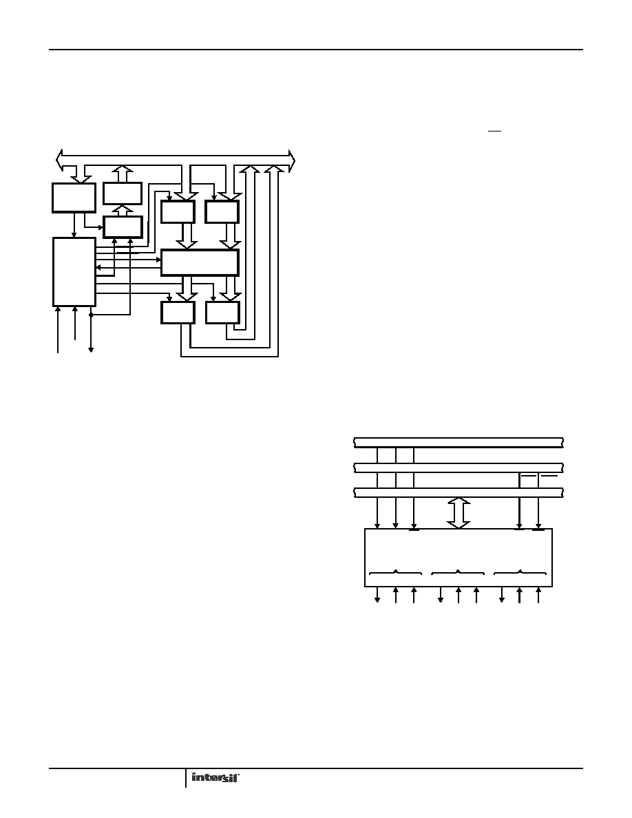
The status register, shown in the figure, when latched,
contains the current contents of the Control Word Register
and status of the output and null count flag. (See detailed
explanation of the Read-Back command.)
The actual counter is labeled CE (for Counting Element). It is
a 16-bit presettable synchronous down counter.
OLM and OLL are two 8-bit latches. OL stands for “Output
Latch”; the subscripts M and L for “Most significant byte” and
“Least significant byte”, respectively. Both are normally referred
to as one unit and called just OL. These latches normally
“follow” the CE, but if a suitable Counter Latch Command is
sent to the 82C54, the latches “latch” the present count until
read by the CPU and then return to “following” the CE. One
latch at a time is enabled by the counter’s Control Logic to drive
the internal bus. This is how the 16-bit Counter communicates
over the 8-bit internal bus. Note that the CE itself cannot be
read; whenever you read the count, it is the OL that is being
read.
Similarly, there are two 8-bit registers called CRM and CRL (for
“Count Register”). Both are normally referred to as one unit and
called just CR. When a new count is written to the Counter, the
count is stored in the CR and later transferred to the CE. The
Control Logic allows one register at a time to be loaded from
the internal bus. Both bytes are transferred to the CE
simultaneously. CRM and CRL are cleared when the Counter
is programmed for one byte counts (either most significant byte
only or least significant byte only) the other byte will be zero.
Note that the CE cannot be written into; whenever a count is
written, it is written into the CR.
The Control Logic is also shown in the diagram. CLK n,
GATE n, and OUT n are all connected to the outside world
through the Control Logic.
82C54 System Interface
The 82C54 is treated by the system software as an array of
peripheral I/O ports; three are counters and the fourth is a
control register for MODE programming.
Basically, the select inputs A0, A1 connect to the A0, A1
address bus signals of the CPU. The CS can be derived
directly from the address bus using a linear select method or
it can be connected to the output of a decoder.
Operational Description
General
After power-up, the state of the 82C54 is undefined. The
Mode, count value, and output of all Counters are undefined.
How each Counter operates is determined when it is
programmed. Each Counter must be programmed before it
can be used. Unused counters need not be programmed.
Programming the 82C54
Counters are programmed by writing a Control Word and
then an initial count.
All Control Words are written into the Control Word Register,
which is selected when A1, A0 = 11. The Control Word
specifies which Counter is being programmed.
By contrast, initial counts are written into the Counters, not
the Control Word Register. The A1, A0 inputs are used to
select the Counter to be written into. The format of the initial
count is determined by the Control Word used.
Write Operations
The programming procedure for the 82C54 is very flexible.
Only two conventions need to be remembered:
1. For Each Counter, the Control Word must be written
before the initial count is written.
2. The initial count must follow the count format specified in the
Control Word (least significant byte only, most significant
byte only, or least significant byte and then most significant
byte).
INTERNAL BUS
CONTROL
LOGIC
CONTROL
WORD
REGISTER
STATUS
LATCH
STATUS
REGISTER
CLK n
GATE n
OUT n
OLM
OLL
CE
CRM
CRL
FIGURE 3. COUNTER INTERNAL BLOCK DIAGRAM
ADDRESS BUS (16)
CONTROL BUS
DATA BUS (8)
I/OR I/OW
WR
RD
CS
A0
A1
A0
8
COUNTER
0
OUT GATE CLK
COUNTER
1
COUNTER
2
OUT GATE CLK
D0 - D7
82C54
FIGURE 4. COUNTER INTERNAL BLOCK DIAGRAM
发布紧急采购,3分钟左右您将得到回复。
相关PDF资料
IDT2308A-4DCI8
IC CLOCK MULT ZD HI DRV 16-SOIC
IDT2309-1HPGGI
IC CLK BUFFER ZD HI DRV 16-TSSOP
IDT2309A-1HPGG
IC CLK BUFFER ZD HI DRV 16-TSSOP
IDT2309B-1HPGGI
IC CLK BUFFER HIGH DRIVE 16TSSOP
IDT23S05-1HDCGI
IC CLK BUFFER PLL HI DRV 8-SOIC
IDT23S05E-1HDCGI8
IC CLK BUFFER PLL HI DRV 8-SOIC
IDT23S08-1HPGI8
IC CLK MULT PLL HI DRV 16-TSSOP
IDT23S08T-1DC
IC CLK MULT PLL ZD 2.5V 16-SOIC
相关代理商/技术参数
ID82C54/+
制造商:未知厂家 制造商全称:未知厂家 功能描述:Analog Timer Circuit
ID82C54-10
制造商:INTERSIL 制造商全称:Intersil Corporation 功能描述:CMOS Programmable Interval Timer
ID82C54-12
制造商:INTERSIL 制造商全称:Intersil Corporation 功能描述:CMOS Programmable Interval Timer
ID82C55A
功能描述:外围驱动器与原件 - PCI PERIPH PRG-I/O 5V 8MHZ 40CDIP IND RoHS:否 制造商:PLX Technology 工作电源电压: 最大工作温度: 安装风格:SMD/SMT 封装 / 箱体:FCBGA-1156 封装:Tray
ID82C55A/+
制造商:未知厂家 制造商全称:未知厂家 功能描述:Peripheral Interface
ID82C55A-5
制造商:HARRIS 制造商全称:HARRIS 功能描述:CMOS Programmable Peripheral Interface
ID82C59A
功能描述:IC CONTROLLER INTERRUPT 28-DIP RoHS:否 类别:集成电路 (IC) >> 接口 - 控制器 系列:- 标准包装:4,900 系列:- 控制器类型:USB 2.0 控制器 接口:串行 电源电压:3 V ~ 3.6 V 电流 - 电源:135mA 工作温度:0°C ~ 70°C 安装类型:表面贴装 封装/外壳:36-VFQFN 裸露焊盘 供应商设备封装:36-QFN(6x6) 包装:* 其它名称:Q6396337A
ID82C59A
制造商:Intersil Corporation 功能描述:Controller IC Package/Case:28-CDIP